

 Semiconductor
Union Cabinet approves Rs.3,700 crore semiconductor plant in Uttar Pradesh
The Union Cabinet on Wednesday approved the setting up of a Rs.3,700 crore semiconductor manufacturing facility close to Uttar Pradesh's Jewar town.
The facility is a joint venture between tech majors HCL and Foxconn.
This is the sixth semiconductor unit that will be set up in India.
#Cabinet approves the establishment of one more semiconductor unit, under India #SemiconductorMission, near #Jewar airport in Yamuna Expressway Industrial Development Authority (YEIDA)
— PIB India (@PIB_India) May 14, 2025
The plant is designed for a capacity of 20,000 wafers per month. The design output capacity is… pic.twitter.com/D2WVxblXgp
In a statement, the Union Cabinet said: "HCL has a long history of developing and manufacturing hardware. Foxconn is a global major in electronics manufacturing. Together they will set up a plant near Jewar airport in Yamuna Expressway Industrial Development Authority or YEIDA."
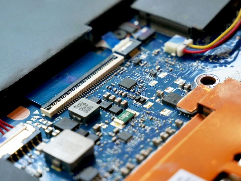
This plant will manufacture display driver chips for mobile phones, laptops, automobiles, PCs, and myriad of other devices that have display.
Details About Proposed Plant In Jewar
As per the government statement, the plant is designed for 20,000 wafers per month.
The design output capacity is 36 million units per month.
"Semiconductor industry is now shaping up across the country. World class design facilities have come up in many states across the country. State governments are vigorously pursuing the design firms," the statement said.
Indian Semiconductor Scenario
Students and entrepreneurs in 270 academic institutions and 70 startups are working on world class latest design technologies for developing new products, the government said in the statement.
Twenty products developed by the students of these academic students have been taped out by SCL Mohali.
"As the country moves forward in semiconductor journey, the eco system partners have also established their facilities in India. Applied Materials and Lam Research are two of the largest equipment manufacturers. Both have a presence in India now. Merck, Linde, Air Liquide, Inox, and many other gas and chemical suppliers are gearing up for growth of our semiconductor industry," read the statement issued by the Indian government.
Support Our Journalism
We cannot do without you.. your contribution supports unbiased journalism
IBNS is not driven by any ism- not wokeism, not racism, not skewed secularism, not hyper right-wing or left liberal ideals, nor by any hardline religious beliefs or hyper nationalism. We want to serve you good old objective news, as they are. We do not judge or preach. We let people decide for themselves. We only try to present factual and well-sourced news.
Support objective journalism for a small contribution.